
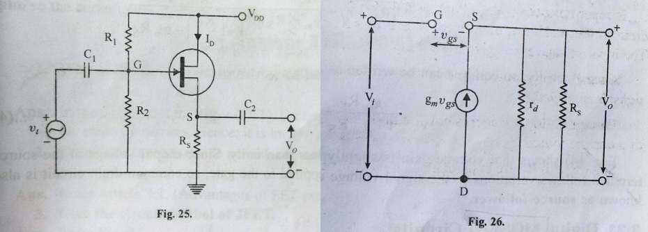
Fig. 25 shows the circuit diagram of common drain jfet amplifier or source follower. The output is taken between the source and the ground.
Expression for common drain jfet amplifier
The equivalent circuit of fig. 25 is shown in fig. 26.
Since rd and RS are in parallel, so their equivalent resistance is given by


Output voltage Vo for common drain jfet amplifier is given by

Using eqn. (1), we get

The input signal applied between gate and drain is represented by the input voltage Vi which is given by


Now, voltage gain (Av) is given by


Since rd >> RS, so eqn. (3) can be written as

Eqn. (4) shows that voltage gain is slightly less than unity. Since output voltage at the source terminal follows variation in the signal voltage applied to the gate, so common drain circuit is also known as source follower.